|
Image: SAMUEL VELASCO
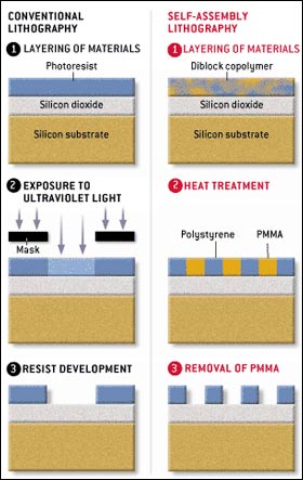
OLD AND NEW: Conventional
lithography exposes a photoresist to ultraviolet light. An
etchant then removes the exposed part of the photoresist.
Self-assembly patterning occurs when a diblock copolymer is
heated, thereby separating the two polymers in the material
into defined areas before the PMMA is etched away. The
template of cyclindrical holes is transferred into the silicon
dioxide before the holes are filled with nanocrystalline
silicon used to store data (steps not
shown). | Self-assembly has become a
critical implement in the toolbox of nanotechnologists. Scientists
and engineers who explore the nano realm posit that the same types
of forces that construct a snowflake--the natural attractions and
repulsions that prompt molecules to form intricate patterns--can
build useful structures--say, medical implants or components in
electronic chips. So far much of the work related to self-assembling
nanostructures has been nothing more than demonstrations in
university laboratories. To go beyond being a scientific curiosity,
these nanotech materials and techniques will have to get from
benchtop to a $2-billion semiconductor fabrication facility.
Four years ago two members of the technical staff at the IBM
Thomas J. Watson Research Center in Yorktown Heights, N.Y., began to
contemplate how they might transform the vision of self-assembly
into a practical reality. The collaborators, Charles Black and
Kathryn Guarini, knew that the grand academic ambitions of making an
entire set of chip circuits from self-assembly had to be set aside.
Instead the best way to begin, they thought, might be to replace a
single manufacturing step. "The idea was that if we could ease the
burden in any of the hundreds of steps to make a chip, we should
take advantage of that," Black says.
They first had to
select what type of molecules might self-construct without
disrupting routine silicon manufacturing practices. Polymers were an
obvious choice. They make up the "resist" used in
photolithography--the material that, once exposed to ultraviolet or
shorter-wavelength light, is washed away to form a circuit pattern.
During the first two years of their quest, the duo spent time
learning about polymers and the optimal temperatures and thicknesses
at which they would self-assemble. They built on the work of Craig
J. Hawker of the IBM Almaden Research Center in San Jose, Calif.,
and that of former IBMer Thomas P. Russell, a polymer scientist at
the University of Massachusetts at Amherst. Both had done research
on how polymers self-assemble on silicon. With this knowledge, Black
and Guarini even started making things. |

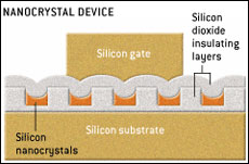
Image: SAMUEL VELASCO
FLASH MEMORY: A layer of
self-assembled silicon nanocrystals is inserted into an
otherwise standard device as part of a novel IBM manufacturing
process. | The two researchers appeared
at conferences, giving presentations about honeycomb patterns that
had self-assembled. But that accomplishment consisted of little more
than PowerPoints, the type of through-the-microscope images found in
abundance at any academic conference on nanotechnology. What would
the nano patterns be good for? How could they be integrated into a
fabrication line? Could they best circuit-patterning techniques that
had already received hundreds of millions of dollars of investment?
Finally, last year, the pair demonstrated how a self-assembled
honeycomb pattern might work in a real manufacturing facility. The
material chosen for the demo was a diblock copolymer, one in which
two polymers--in this case, polystyrene (Styrofoam) and
polymethylmethacrylate (Plexiglas, or PMMA)--are tied together by
chemical bonds. When spun onto the surface of a rotating silicon
wafer, the two polymers separate, as if they were oil and water.
Although the molecules stretch out, the chemical bonds keep them
attached. Subsequent heat treatment exacerbates this elongation. In
the end, PMMA ends up concentrated in small cylinders surrounded on
all sides by the polystyrene. The diblock copolymer thus forms on
its own into a nearly complete honeycomblike template.
To finish creating the 20-nanometer-wide pores, an organic etching
solvent removes the PMMA. A subsequent etching step transfers
the same honeycomb pattern into an underlying layer of more
robust silicon dioxide. Then a coating of amorphous silicon
gets deposited across the surface of the wafer. A gas etches
away the silicon except for that deposited in the holes. All
that is left are nanocrystalline cylinders surrounded by silicon
dioxide. The final steps place an insulating layer and a block
of silicon atop the structure, the block forming a "gate" that
turns the electronic device off and on. Black and Guarini's
honeycomb results in a nanostructure that is part of a working
flash-memory device, the kind that retains digital bits even
when a camera or a voice recorder is turned off. The nanocrystalline
cylinders form capacitors where data are stored.
Manufacturing engineers are leery of introducing new technologies
unless a researcher can make a very good case for their adoption.
Self-assembly potentially fits the bill. Creating closely spaced
holes for a flash memory would prove exceedingly difficult with
ordinary lithographic and deposition methods. Forming nanocrystals
using conventional techniques creates elements of different
sizes that are all jumbled together. In contrast, the self-assembled
nanocrystals are evenly spaced and of uniform size, improving
their durability and their capacity to retain a charge while
allowing the cylinders to shrink to smaller than 20 nanometers.
The IBM demonstration served as proof of principle in the strictest
sense of the expression. The company has not made commercial
flash memories for years, so the invention could not be applied
immediately to improve its own manufacturing operations. But
the nanocrystals enabled the pair of researchers to flaunt this
type of nano patterning. "Politically in the company maybe
it wasn't the smartest demonstration we could have done, but
everybody was supportive and could see the power of the technology,"
Black says.
The understanding gained of how to integrate nanomanufacturing
with conventional chipmaking may provide new approaches to fabricating
other IBM electronic components. Making holes and filling them
could create "decoupling" capacitors recessed into
the chip substrate that smooth out fluctuations in the power
supplied to a chip.
Using a variant of nano patterning, a self-assembling polymer
could also create tiny, finger-shaped silicon protrusions sticking
up from the underlying substrate. These fingers would constitute
the "channel" in a transistor through which electrons
flow--but one in which electrons flow vertically instead of
across a chip, as in today's devices. The gate to turn the transistor
off and on could encircle the silicon finger. The geometry might
prevent electrons from "tunneling," or leaking, through
the channel when the transistor is in the off state, a constant
threat when feature sizes become very small.
Ultimately, self-assembly might play a much bigger role in fashioning
electronic circuits. But the incrementalist approach of Black
and Guarini may represent the most promising way to get nanotechnology
adopted as a real manufacturing tool. "The greatest excitement
is that these materials aren't just in the polymer-science laboratory
anymore," Black says. A small step for small manufacturing.
|

